Home⁄ Facilities⁄ Instruments⁄ User Instruments⁄ Electron and Optical Microscopy⁄ Zeiss Sigma 500 Scanning Electron Microscope
Zeiss Sigma 500 Scanning Electron Microscope
Bard Hall SB58C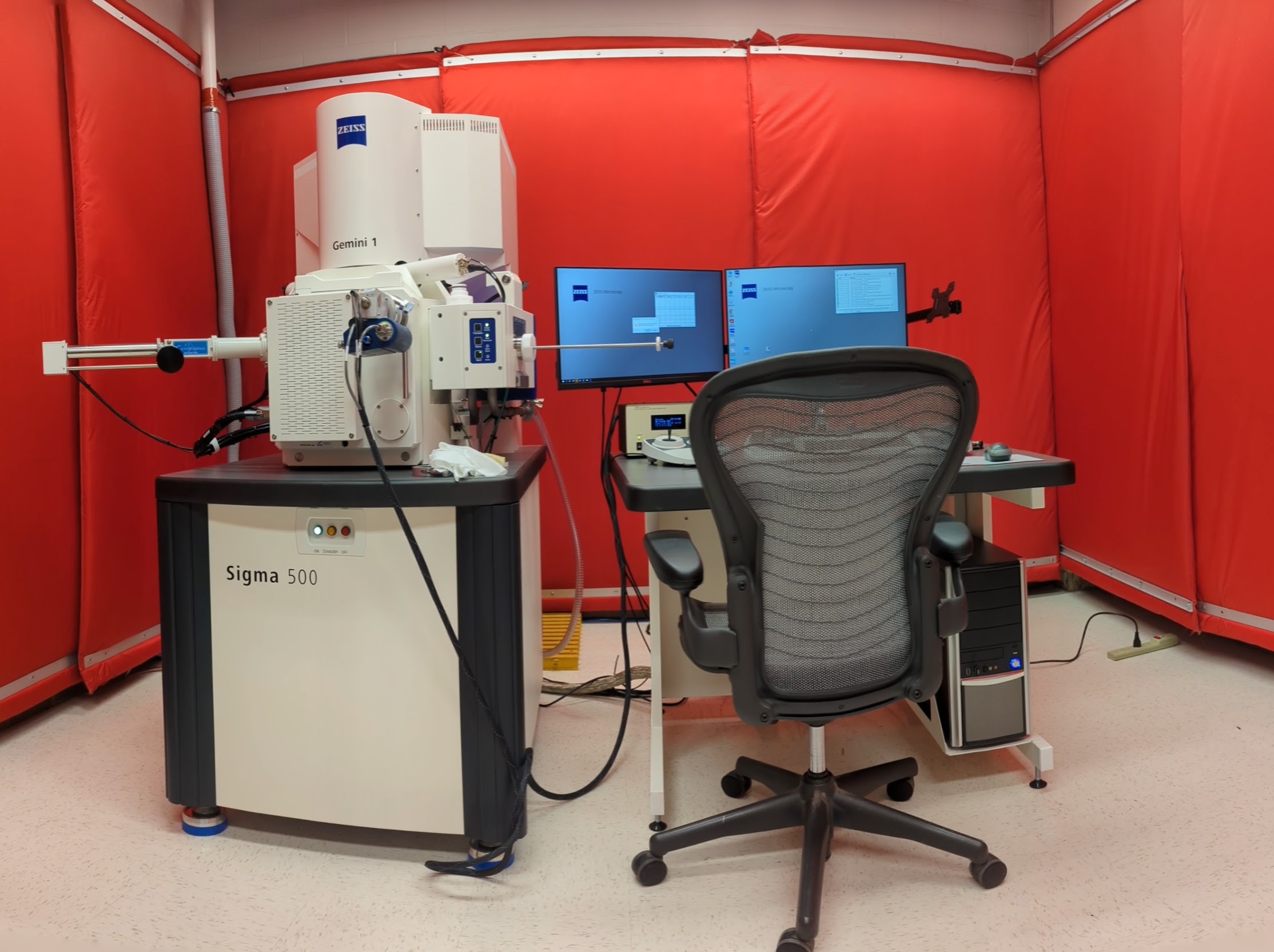
The Zeiss Sigma 500 Scanning Electron Microscope (SEM) takes the best capabilities of the Keck SEM and enhances them. It is primarily designed to provide high resolution imaging at low and ultra-low accelerating voltages (3keV down to 200eV) using the in-lens secondary electron detector. In this voltage regime contrast from the sample surfaces is optimized. Other imaging detectors include a scintillating backscatter detector and standard Everhart-Thornley secondary electron detector.
In addition to electron imaging, the Sigma is equipped with an electron backscatter diffraction detector (EBSD) and X-ray spectrometer for energy-dispersive-X-ray-spectroscopy (EDS). More information about these techniques can be found below. A load-lock enables samples to be quickly loaded and unloaded. For further questions please contact Philip Carubia (pmc228@cornell.edu or 607-255-6757).
To request training on this instrument, complete this form.
EDS/EDX
Energy-dispersive X-ray spectroscopy (EDS) is a technique used in conjunction with scanning electron microscopy (SEM) to characterize the elemental composition of materials. By directing an electron beam onto a sample surface, the interaction between the electrons and the atoms generates characteristic X-rays. EDS detects and quantifies these X-rays, allowing for the identification and mapping of elements present in the sample. This information is crucial for understanding the chemical composition, phase distribution, and elemental distribution within materials, making EDS an essential tool for various scientific and industrial applications, including materials analysis, geological studies, and semiconductor device fabrication.
EBSD
Electron Backscatter Diffraction (EBSD) is a microscopy technique used to analyze the crystallographic orientation and microstructure of materials. By directing an electron beam onto a sample surface within a scanning electron microscope (SEM), EBSD captures diffraction patterns produced by backscattered electrons. These patterns are then analyzed to determine the crystallographic orientation, grain boundaries, and other microstructural features of the material. EBSD is valuable for understanding the relationship between structure and properties in a wide range of materials, including metals, ceramics, and geological samples, making it a powerful tool for materials science research and industrial applications.

Philip Carubia
607/255-6757
pmc228@cornell.edu
Bard Hall, Room SB-56
Secondary Contact

Malcolm (Mick) Thomas
607/255-0650
mt57@cornell.edu
Duffield Hall, Room 150