Home⁄ Facilities⁄ Instruments⁄ User Instruments⁄ Electron and Optical Microscopy⁄ Zeiss LEO 1550 FESEM (Keck SEM)
Zeiss LEO 1550 FESEM (Keck SEM)
Clark Hall F3
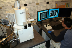
Scanning electron microscope (SEM) imaging at very high resolution (1 nm at 20 keV and 2.5 nm at 5 keV) is possible with certain types of specimens. Its superb performance, particularly at low accelerating voltages (i.e., 0.5 to 3 kV), makes it especially suitable for imaging the surface detail of polymeric, biological, and other low-density materials. An in-lens secondary electron detector enables a very short working distance and responds to the lowest voltage secondary electrons. Transmission Electron Imaging TEM grids may be used in a special stage in conjunction with a detector below the specimen to obtain transmitted electron images.
To request training on this instrument, complete this form.

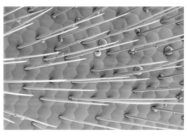
Secondary electron image of a bee’s eye
Primary Contact

Malcolm (Mick) Thomas
607/255-0650
mt57@cornell.edu
Duffield Hall, Room 150

Malcolm (Mick) Thomas
607/255-0650
mt57@cornell.edu
Duffield Hall, Room 150
Secondary Contact

Mariena Silvestry Ramos
607/255-6272
msilvestry@cornell.edu
PSB Room G-07

